- To analyze time-domain structure, use delayed conjugate multiplication and observe the resulting phase.
- To distinguish between ordinary QPSK and π/4-QPSK, use the fourth-power method.
Example 1: Verifying the Time-Domain Structure
Based on patents and papers, I hypothesized that:
- The uplink baseband sampling rate is 60 MHz.
- The STF consists of eight repetitions of a 128-sample sequence plus a 48-sample CP.
- Each OFDM symbol consists of a 1024-sample symbol body plus a 48-sample CP.
Alternatively, the OFDM symbol can be viewed as having a 24-sample cyclic prefix and a 24-sample cyclic postfix, as described in patent US12003350.
To verify this, delayed conjugate multiplication can be applied to the IQ samples:
- Use a 128-sample delay to detect the eight repeated STF sequences.
- Use a 1024-sample delay to detect the CP and OFDM symbol structure.
Since the signal is multiplied by a delayed version of itself, this method is insensitive to carrier frequency offset.
128-Sample Delayed Conjugate Multiplication (Unless otherwise stated, Style 1 packets are used as examples.)

The result clearly shows the eight repetitions of the 128-sample sequence. It can also be seen that the first sequence has a 180° phase difference relative to the other seven repetitions.
1024-Sample Delayed Conjugate Multiplication

The result confirms that the assumed CP length and OFDM symbol length are correct. The CP region produces a constant phase difference in the delayed conjugate multiplication result.
This property can be used to:
- Locate OFDM symbol boundaries.
- Estimate the fractional carrier frequency offset.
Identifying QPSK Using the Fourth-Power Method
After obtaining the frequency-domain subcarrier symbols, plot their phases. As an example, consider the first OFDM symbol of a Style 1 packet.

The constellation appears to contain only four possible phases, suggesting QPSK modulation. To verify this, plot the phase of the symbols after raising them to the fourth power.

The points collapse near to a single line, it confirms that the original modulation contains only four phase states.
If that line has a non-zero slope, it can also be used to estimate and compensate sampling phase errors, either:
- in the time domain, or
- on a per-subcarrier basis in the frequency domain.
Detecting π/4-QPSK
An interesting result appears when the fourth-power phase is plotted for the second OFDM symbol of a Style 1 packet.

Two groups of subcarriers converge to a phase that differs by 180° from that of most other subcarriers. This indicates that these subcarriers are rotated by 45° (π/4) relative to the others, because:
45° × 4 = 180°
The corresponding constellation diagrams were shown in the previous post.
Connection to Starlink Pilot Sub-Bands
A reasonable hypothesis is that these special subcarrier regions correspond to pilot subcarriers embedded within the data symbols. This is consistent with the PILOT SUB-BANDS shown in the well-known Starlink patent US12003350B1.

The parameter examples described in the patent match the observations reported in the previous post remarkably well:
“For example, the offset can be a 16 tone (another name for subcarrier) pilot sub-band offset from the band edge. ”
“a burst 1622 can include N subcarriers 1622 including a first 16 tone (subcarrier) pilot sub-band offset from a band edge 1624 at a low end of the frequency spectrum and a second 16 tone pilot sub-band offset from another band edge 1636 at a high end of the frequency spectrum.”
]]>(Unless otherwise stated, all analysis in this post is performed on the first OFDM symbol following the STF within each packet.)
First, I would like to correct a previous conclusion: In “Starlink uplink signal analysis (3): demodulation is successful”, I thought that the two OFDM symbols following the full-bandwidth STF were likely training sequences similar to the LTF in Wi-Fi. After analyzing many more packets, I now believe this is probably incorrect. The OFDM symbols following the STF frequently appear to contain actual data (or signaling information) rather than fully known pilot patterns like a Wi-Fi LTF. The packet structure is therefore updated as shown below.

The packet previously classified as Style 1 (the structure shown above) contains a single 252-subcarrier RU (-260 to -9, 14.766 MHz).

The demodulated constellation of its first OFDM symbol is shown below.

After hard decision, the real and imaginary bits are obtained as follows:
- Mapping: 1 to 0, -1 to 1
- Includes the usual 90° phase ambiguity
style1_sub1_ru1_sym1 real part
1 0 1 1 0 0 1 1 0 1 0 1 1 1 1 0 1 1 0 1 0 1 0 1 0 1 1 0 1 0 1 0 1 0 0 0 0 0 1 1 0 0 1 0 1 1 1 0 1 0 0 0 1 0 1
1 1 0 1 1 0 1 1 0 0 1 0 0 0 1 0 1 1 1 1 0 0 1 1 0 1 1 1 0 0 0 1 0 1 1 1 1 1 0 1 0 1 1 0 0 1 1 0 1 1 0 1 1 0 0
1 0 1 1 0 1 0 0 1 1 0 0 0 0 0 0 0 0 1 0 0 1 0 1 1 0 0 1 0 1 0 0 1 0 0 0 0 0 1 0 1 1 0 1 0 0 0 0 0 0 0 1 0 0 0
1 1 1 1 1 0 1 0 0 0 0 0 0 0 1 0 0 0 1 1 0 1 1 0 0 0 1 1 1 1 0 0 1 1 0 0 0 0 0 1 0 1 01 1 0 1 0 1 0 1 0 1 1 0
1 1 0 1 1 0 0 0 0 0 1 1 0 0 1 1 1 1 1 0 1 0 0 0 1 0 1 1 1 1 0 1
style1_sub1_ru1_sym1 imag part
0 1 1 1 0 0 1 0 0 0 0 1 1 1 0 0 0 1 0 1 0 0 1 0 1 1 1 0 0 1 0 1 1 0 0 1 0 0 1 0 0 0 0 0 1 1 0 0 1 1 1 0 1 1 0
1 0 1 1 1 1 0 1 1 0 0 0 1 0 0 1 1 0 1 0 0 1 0 0 1 0 0 0 1 0 1 0 1 0 0 0 1 1 0 1 0 1 1 1 1 1 1 0 1 1 1 1 1 0 0
1 0 0 1 1 1 0 0 1 0 1 0 0 0 0 0 1 1 0 1 0 1 0 0 1 1 0 1 0 1 1 0 1 0 1 0 0 1 0 1 0 1 0 1 1 1 0 0 1 1 0 0 0 0 0
0 1 1 0 1 1 1 1 0 1 1 1 0 0 0 1 0 1 0 0 1 0 0 1 0 0 0 1 0 1 1 1 1 1 0 0 0 0 1 1 1 0 10 0 0 0 0 1 0 1 0 0 0 1
1 1 0 1 0 1 1 0 0 0 1 0 0 0 0 1 1 1 0 0 1 1 0 0 1 1 0 1 0 0 0 1
In the first RU of a Style 5 packet (also a 252-subcarrier RU, 14.766 MHz), I obtained exactly the same bit sequence. (A Style 5 packet also contains a second, wider RU (8 to 507, 29.53 MHz). )

The figure below shows the sliding correlation result between the hard-decision sequences of the 252-subcarrier RU in the Style 5 packet and the corresponding RU in the Style 1 packet.

The correlation peak is exactly: 2 × 252 = 504 indicating that the two hard-decision complex sequences are identical.
The second OFDM symbol of the Style 1 packet contains an unusual modulation structure: Most of the 252 subcarriers use QPSK. However, the following subcarrier groups: 17 to 24 and 229 to 236 for a total of: 2 × 8 = 16 subcarriers (or 2 × 0.469 MHz) use a QPSK constellation rotated by 45° (π/4).
The constellation diagrams of these two modulation types are shown in the figures below.


This modulation structure also appears in Style 3 packets. In fact, Style 3 packets contain an even more complicated modulation pattern.

Within the 504-subcarrier RU (upper edge of the channel) of the style 3 packet: The first 126 subcarriers (7.38 MHz) have the same modulation structure as the first 126 subcarriers of the Style 1 packet.
- Subcarriers 17 to 24 use π/4-QPSK.
- The remaining subcarriers use standard QPSK.
More interestingly, the further: 504 − 126 = 378 subcarriers (22.15 MHz) appear to use 16-QAM rotated by a fixed angle.
The three modulation types present in this 504-subcarrier RU of the style 3 packet are illustrated in the three constellation plots below.


Although similar modulation structures are observed in both Style 1 and Style 3 packets, the hard-decision QAM symbol sequences from the corresponding subcarriers show no significant correlation peaks. This suggests that the transmitted bit contents are different.
An especially interesting result was found for the narrowband Style 7 packets. These packets contain a 63-subcarrier RU (3.69 MHz) located near the lower edge of the channel.

After examining four such packets, I found that the hard-decision QPSK contents of their first OFDM symbols were completely identical.

The figure below shows the sliding correlation results among the hard-decision complex sequences from four Style 7 packets. The correlation peak is exactly: 2 × 63 = 126 indicating perfect alignment.

After hard decision, the real and imaginary bits are obtained as follows:
- Mapping: 1 to 0, -1 to 1
- Includes the usual 90° phase ambiguity
style7_sub1_ru1_sym1 real part
1 1 1 1 1 1 0 1 1 1 1 0 0 0 1 0 1 0 0 0 1 1 0 1 0 0 0 1 1 1 0 0 1 0 1 0 1 1 0 1 1 1 1 0 0 1 0 1 1 0 0 1 0 0 1 0 1 1 1 1 0 0 1
style7_sub1_ru1_sym1 imag part
0 0 1 0 0 0 1 0 0 1 1 1 1 1 0 1 1 0 1 1 0 0 1 1 1 0 1 0 0 0 0 1 1 1 0 1 0 1 0 1 1 0 0 1 0 1 0 1 0 1 1 1 1 1 0 0 0 0 1 0 1 1 1
]]>The observed numbers of active subcarriers per RU are:
- 63
- 189 (3 × 63)
- 252 (4 × 63)
- 441 (7 × 63)
- 504 (8 × 63)
All signals were captured from the first uplink channel, centered at 14 GHz + 31.25 MHz.
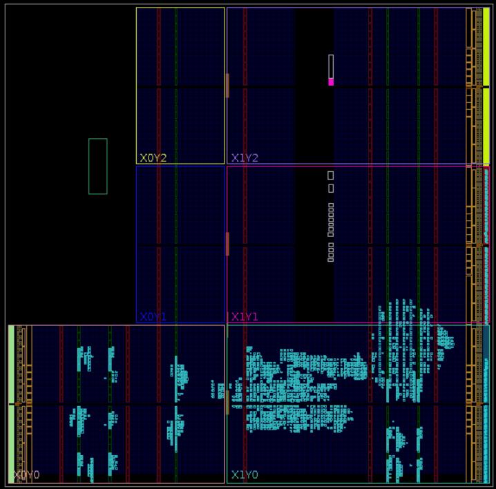
I identified eight packet types (shown in the figure), each corresponding to a particular OFDMA RU allocation pattern. One important observation is that all OFDM symbols within the same packet use the same RU allocation pattern.


I would like to invite others to help solve this Starlink uplink OFDMA puzzle.
Known facts and current hypotheses are as follows.
- The fractional carrier frequency offset (fractional subcarrier spacing offset) has already been estimated and corrected.
- The integer carrier frequency offset (integer multiples of the subcarrier spacing) still requires estimation and is currently uncertain.
This is because the exact Starlink RU-to-subcarrier mapping is unknown. Even if an RU is shifted by several subcarriers, we can still observe the constellation on those subcarriers.
In addition, the Starlink terminal performs frequency hopping across eight uplink channels, each 62.5 MHz wide. This is likely related to satellite and beam frequency planning. We also do not know whether the inherent frequency offset changes when the terminal hops back to the first channel, although the receive frequency of my AD9361 remains fixed throughout the experiment.
Because of this unknown integer frequency offset, there are two possible ways to align the frequency-domain results of the eight packet types:
- Align the DC spikes.
- Align the points where the spectrum edges fall to the noise floor.
Method 2 is used here because it is unclear whether the frequency offset remains constant each time the terminal returns to the first channel. This is also why the DC spikes appear at slightly different locations in the figure.
The measured RU edge subcarrier indices and DC spike indices for the eight packet types are listed below. The subcarrier index range is −512 to 511.
If only one pair of RU edge indices is present, the packet contains one RU. If two pairs are present, the packet contains two RUs.
pkt style 1
RU edge subcarrier indices: -260   -9
DC index: -2

pkt style 2
RU edge subcarrier indices: -508   -7    10   261
DC index: -1

pkt style 3
RU edge subcarrier indices: 67   507
DC index: -1

pkt style 4
RU edge subcarrier indices: -508   -320
DC index: 8

pkt style 5
RU edge subcarrier indices: -260   -9    8   507
DC index: -4

pkt style 6
RU edge subcarrier indices: -318   -130
DC index: 9

pkt style 7
RU edge subcarrier indices: -508   -446
DC index: -1

pkt style 8
RU edge subcarrier indices: -508   -5
DC index: -1
Who is ready to take on the challenge?
]]>
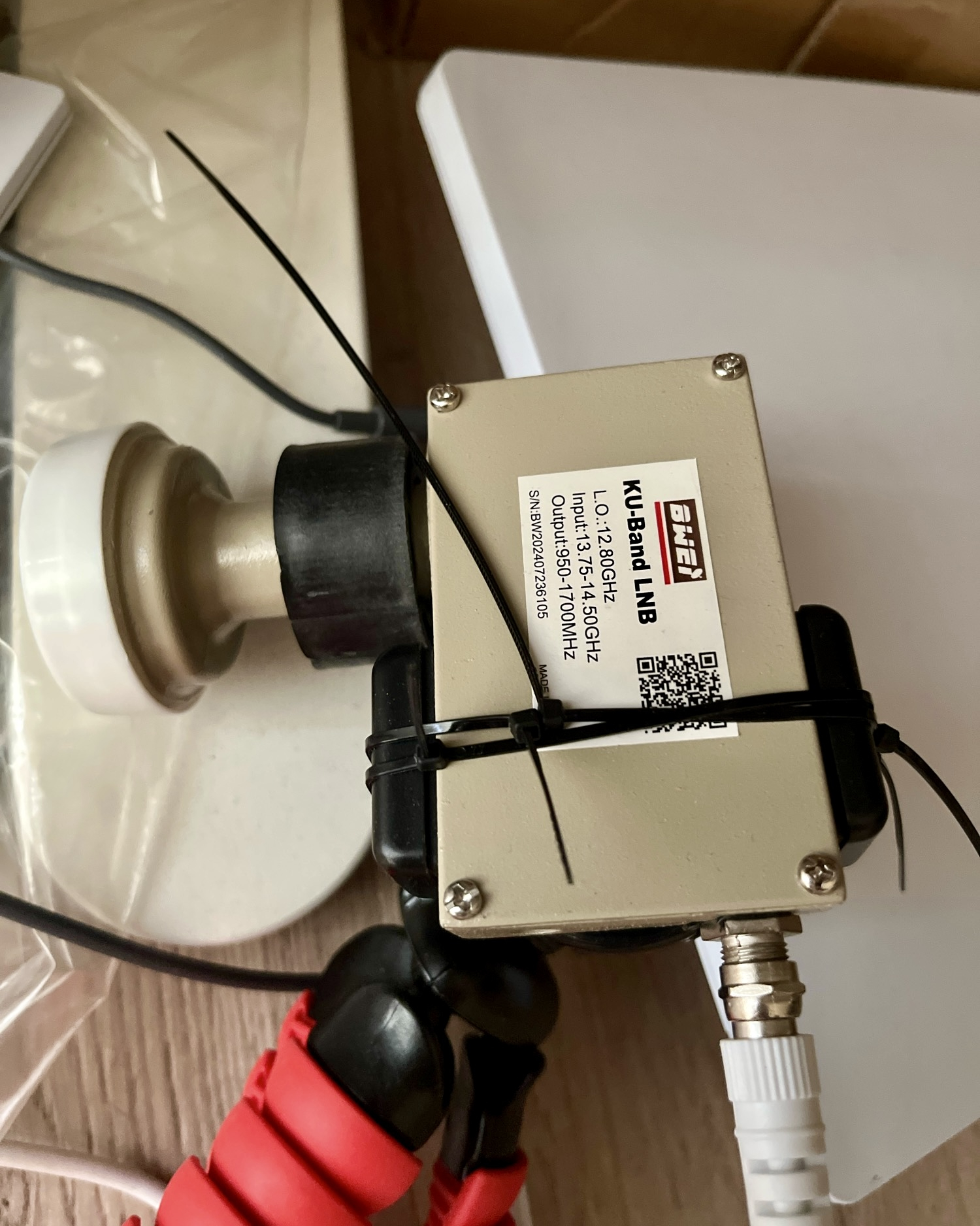
As described in this paper (https://arxiv.org/abs/2304.09535), a 14 GHz LNB can easily capture transmitted signals from Starlink terminals. Thanks to Starlink’s rapid expansion and widespread adoption across Europe, I was able to perform this experiment myself (Yes I have one).
Just search “Ku band LNB 12.8GHz” on Aliexpress.
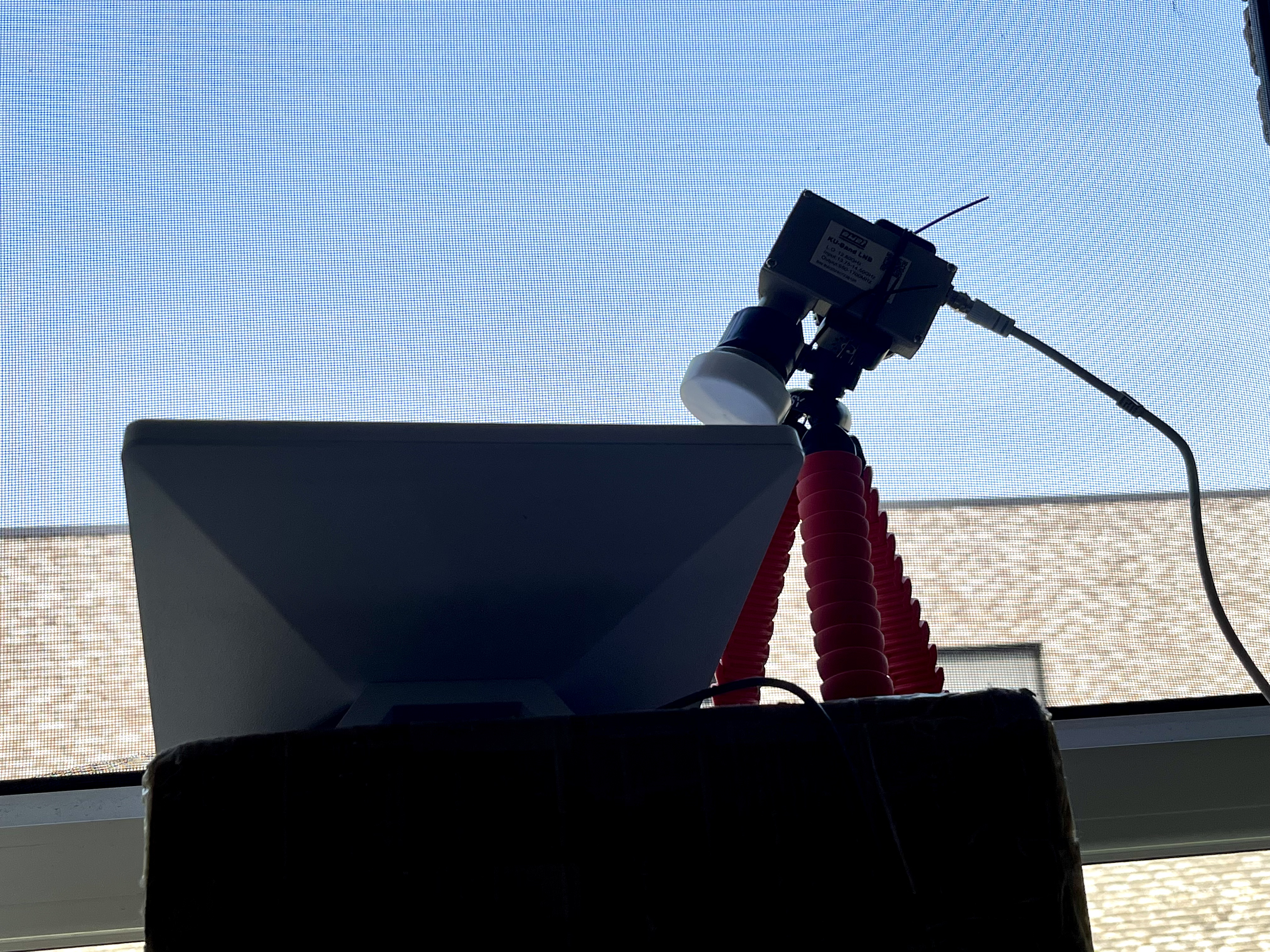
The 60MHz uplink baseband sampling rate of Starlink is fully within the capabilities of the AD9361. Conveniently, I had several AD9361-based SDRs available (thanks to supporters). Although streaming a 60Msps signal in real time over a 1Gbps Ethernet link is not feasible, it is still possible to trigger a capture, store the packet inside the FPGA, and then transfer it out at a slower rate. This allowed me to obtain complete packets with the full 60 MHz bandwidth.
One frequently occurring ultra-short uplink packet is shown below.
The IQ capture:

The analysis result:

The Starlink uplink baseband sampling rate is 60 Msps.
The first 48 + 128 × 8 = 1072 samples (17.8667 μs) form the STF (Short Training Field). It consists of a 48-sample cyclic prefix (CP) followed by eight repetitions of a 128-sample sequence across the full bandwidth. The first 128-sample sequence has a 180° phase offset relative to the other seven sequences.
The next two 1072-sample sections are OFDM symbols corresponding to the LTF (Long Training Field). Each consists of a 48-sample CP and a 1024-sample symbol body (FFT length = 1024). Both use a scheme similar to the Cyclic Shift Diversity (CSD) employed in Wi-Fi, with a delay equal to half of the CP length, i.e., 24 samples.
Only 252 subcarriers are active in this sample of LTFs, occupying just one-quarter of the total bandwidth.
Another interesting observation is that the carrier frequency offset (CFO) continuously changes across the three signal segments (STF, LTF1, and LTF2). This may be caused by hardware warm-up drift, or it may be part of a Doppler pre-compensation mechanism.
This becomes particularly interesting when compared with Wi-Fi uplink OFDMA (client to access point), which was introduced since Wi-Fi6/802.11ax.
Starting from Wi-Fi 6, multiple users can transmit simultaneously to an access point through OFDMA, with different users occupying different resource units (RUs, subbands). However, due to legacy compatibility requirements, before the actual OFDMA uplink transmission begins, every user transmits several identical full-bandwidth legacy fields (L-STF, L-LTF, L-SIG, RL-SIG, etc.), wasting both time and energy. Only afterward do users transmit data within their assigned RU/subband.
Starlink has no such legacy burden. The terminal transmits only a single full-bandwidth STF. After that, time-frequency resources are already divided into subbands (one-quarter bandwidth in this example) and further separated using CSD. This allows the satellite to separate signals from different terminals at a much earlier stage and greatly reduces potential contention and collisions during initial uplink access. It is a very clean and efficient design.
The successful demodulation procedure was:
- Estimate the CP and FFT lengths (with the help of publicly available information, such as papers on the downlink signal).
- Perform the FFT from the expected offset to take a look.
- Estimate and compensate the carrier frequency offset (integer times of the subcarrier width).
- Estimate and compensate the carrier frequency offset (fractional times of the subcarrier width), which is interestingly different for STF, LTF1, and LTF2
- Plot the constellation.
Because my receiver was located very close to the terminal, the channel can be approximated as AWGN, making channel estimation and equalization unnecessary.
The FFT results and demodulated constellations for the two LTF symbols are shown below.


English abstract:
Pilot Assisted Block Transmission (PABT)
JIAO Xianjun (Communication and Information system)
Directed by Prof. XIANG Haige
Abstract:
Pilot Assisted Block Transmission (PABT) is a transmission scheme suitable for broadband wireless communication. In this scheme, data are grouped into separated blocks, in which pilot are inserted. Receiver gets channel state information (CSI) based on observation of received pilot in real time and makes demodulation according to CSI. Considering the time variety and frequency selective characters of broadband wireless channel in modern wireless broadcasting, mobile and wireless network system, PABT is a reasonable choice. In this thesis, a uniform signal framework of PABT is summarized based on investigations of existing broadband systems, and two kinds of PABT system are presented under the framework: pilot and data are in time division multiplexing form; pilot and data are in frequency division multiplexing form. Researches on key technologies and systems of PABT are carried out. This thesis include:
-
A uniform signal framework of PABT is summarized, and many signal formats are presented under the framework. Those formats are classified into two kinds: pilot and data are in time division multiplexing form; pilot and data are in frequency division multiplexing form. In the first kind, there are four basic formats: “PN (Pseudo Noise) pilot + SC (Single Carrier) data”, “PN pilot + OFDM data”, “OFDM pilot + SC data”, “OFDM pilot + OFDM data”. The second kind is referred to traditional OFDM systems with frequency domain pilot in fact. In addition, with different form of guard interval, for example CP (Cyclic Prefix), ZP (Zero Padding)…, more signal formats can be created. The formats include not only most existing systems but also new systems. Key technologies of PABT are discussed under the framework, which are: Channel Estimation (CE), Euqalization, Iterative Interference Canceling and guard interval signal design for higher efficency.
-
All kinds of CE algorithm are studied and summarized. The procedure of CE is separated into three steps: pre-process, channel estimate, post-process. Two algorithms of estimating time domain channel impulse response (CIR) are studied, which are move correlation and circular correlation. Two algorithms of estimating channel frequency response are also studied, which are frequency domain estimation after “cut-and-add” and zero padding frequency domain estimation. A new CE algorithm based on PN pilot with circular correlation is proposed. The new CE algorithm has almost the same performance with existing algorithm, but the complexity of new algorithm is much lower than that of existing algorithm. A new post-process algorithm is also proposed, which leads to visible performance gain compared to CE without post-process. The idea of new post-process algorithm is that certain number of strong path is reserved and other paths are removed as noise. The performance of new post-process algorithm has no “floor” phenomenon, which is a drawback of exsisting algorithm.
-
Time domain equalization (TDE) and frequency domain equalization (FDE) of CP/ZP block are summarized and studied. TDE and FDE are proved to be equivalent. Two MMSE (Minimum Mean Square Error) FDE algorithms are studied: direct FDE and FDE after “cut-and-add” pre-process. Quasi-MMSE FDE alogrithms is studied. The complexity of quasi-MMSE algorithm is much lower than that of strict-MMSE algorithm, and performance degradation is only about 0.1dB, when 7, [171 133], 1/2 convolution code and random interleaver are employed.
-
Iterative interference canceling algorithm is studied in the situation that pilot and data are in time division multiplexing form and without guard interval. A simplified algorithm is proposed for situation where pilots are invariant. As applications of iterative interference canceling, “OFDM pilot + SC data” and “OFDM pilot + OFDM data” PABT system is studied. Simulation shows that two systems are suitable for broadband wireless communication with high mobility (moving speed 130km/h; doppler frequency 100Hz in 800MHz band). When CIR is short, for example DVB-T portable reception channel, performance of new systems can approach that of reference system with guard, which needn’t interference canceling, and new systems have higher bit rate.
-
In the situation that pilot and data are in time division multiplexing form, a new PP-OFDM (Pilot Postfixing - OFDM) scheme is proposed as a modification of traditional CP-OFDM. Replacing CP signal with PP signal in guard interval ensures that PP-OFDM has higher efficiency of utilizing pilot power than CP-OFDM. ZP-OFDM can be derived from PP-OFDM. Pilot power allocation is studied in PP-OFDM, and analytic result is derived. When 1/4 guard interval is adopted, PP-OFDM has about 1dB performance gain compared with CP-OFDM.
Key words:
PABT (Pilot Assisted Block Transmission); OFDM (Orthogonal Frequency Division Multiplexing); Channel Estimation; Frequency Domain Equalization; Iterative Interference Canceling
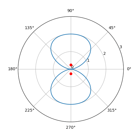
]]>Since the double-slit interference pattern can be moved by altering the light delay in one of the slits, you must have realized that if we can control the delay/phase of the radio signal before it leaves the antenna, we might be able to direct the beam where we want it. Indeed, this is the basic principle of beamforming. By applying delay/phase to the signal per antenna, we can shape the beam as desired. Next, let’s start from a simple case: applying phases of 0 and π to the the two rod antennas in the previous article. Run the following command:
python3 -c "from beamforminglib import *; ant_array_beam_pattern(freq_hz=2450e6, array_style='linear', num_ant=2, ant_spacing_wavelength=0.5, beamforming_vec_rad=np.array([0, np.pi]))"
The figure on the right is obtained by the above command, with the left showing the original beam.
Similar to the double-slit interference case, in this case, there is no signal at 0 degrees (to the right).
Since the beam can be directed towards 0 and 90 degrees by applying phases (0 and π) to the two antennas, wouldn’t it be possible to do beam scanning by using some intermediate phase values? The answer is YES. The following command demonstrates beam scanning by continuously changing the phase of the 2nd antenna from -π to π with step size π/8 while keeping the phase of the 1st antenna 0:
python3 test_linear2_bf_scan.py
If you open the test_linear2_bf_scan.py, you will find: it calls the same python function ant_array_beam_pattern continuously and gives a series of phase (-π to π with step size π/8) to the 2nd antenna via the 2nd element of the argument beamforming_vec_rad, which are listed in the following table:
| time | phase ant0 | phase ant1 |
|---|---|---|
| 0 | 0 | -π |
| 1 | 0 | -7π/8 |
| 2 | 0 | -6π/8 |
| 3 | 0 | -5π/8 |
| 4 | 0 | -4π/8 |
| 5 | 0 | -3π/8 |
| 6 | 0 | -2π/8 |
| 7 | 0 | -1π/8 |
| 8 | 0 | 0 |
| 9 | 0 | 1π/8 |
| 10 | 0 | 2π/8 |
| 11 | 0 | 3π/8 |
| 12 | 0 | 4π/8 |
| 13 | 0 | 5π/8 |
| 14 | 0 | 6π/8 |
| 15 | 0 | 7π/8 |
To generate a narrower beam and the scanning, the number of antennas in the array can be extended from 2 to 8. The antenna spacing is still half of the wavelength. All antennas are in one line. This kind of array topology is called ULA: Uniform Linear Array. Regarding the phasing scheme: the 1st antenna’s phase is kept 0, and starting from the 2nd antenna the phasing step sizes are π/8, 2π/8, 3π/8, …, 7π/8. You can check test_linear8_bf_scan.py to see the exact beamforming phase vector with 8 elements (argument beamforming_vec_rad). The corresponding command and scanning figure are:
python3 test_linear8_bf_scan.py
The corresponding phases per antenna are:
| time | ant0 | ant1 | ant2 | ant3 | ant4 | ant5 | ant6 | ant7 |
|---|---|---|---|---|---|---|---|---|
| 0 | 0 | -π | -2π | -3π | … | … | … | -7π |
| 1 | 0 | -7π/8 | -2*7π/8 | -3*7π/8 | … | … | … | -7*7π/8 |
| 2 | 0 | -6π/8 | -2*6π/8 | -3*6π/8 | … | … | … | -7*6π/8 |
| 3 | 0 | -5π/8 | -2*5π/8 | -3*5π/8 | … | … | … | -7*5π/8 |
| 4 | 0 | -4π/8 | -2*4π/8 | -3*4π/8 | … | … | … | -7*4π/8 |
| 5 | 0 | -3π/8 | -2*3π/8 | -3*3π/8 | … | … | … | -7*3π/8 |
| 6 | 0 | -2π/8 | -2*2π/8 | -3*2π/8 | … | … | … | -7*2π/8 |
| 7 | 0 | -1π/8 | -2*1π/8 | -3*1π/8 | … | … | … | -7*1π/8 |
| 8 | 0 | 0 | 0 | 0 | 0 | 0 | 0 | 0 |
| 9 | 0 | 1π/8 | 2*1π/8 | 3*1π/8 | … | … | … | 7*1π/8 |
| 10 | 0 | 2π/8 | 2*2π/8 | 3*2π/8 | … | … | … | 7*2π/8 |
| 11 | 0 | 3π/8 | 2*3π/8 | 3*3π/8 | … | … | … | 7*3π/8 |
| 12 | 0 | 4π/8 | 2*4π/8 | 3*4π/8 | … | … | … | 7*4π/8 |
| 13 | 0 | 5π/8 | 2*5π/8 | 3*5π/8 | … | … | … | 7*5π/8 |
| 14 | 0 | 6π/8 | 2*6π/8 | 3*6π/8 | … | … | … | 7*6π/8 |
| 15 | 0 | 7π/8 | 2*7π/8 | 3*7π/8 | … | … | … | 7*7π/8 |
(To be continued …)
]]>The commonly used wavelength of red light in double-slit interference is approximately 620 to 750 nanometers, corresponding to a frequency range of 484 to 400 THz. Here, we take a wavelength of 700 nanometers, which corresponds to a frequency of 428.6 THz. In double-slit interference experiments, it is generally required that the distance between the two slits be less than 1mm. Here, we take 0.5mm, which is about 714 times the wavelength. In this setup, the two slits correspond to the two antennas in our model. To set these parameters in our simulation code, the command is as follows:
python3 -c "from beamforminglib import *; ant_array_beam_pattern(freq_hz=428.6e12, array_style='linear', num_ant=2, ant_spacing_wavelength=714, angle_vec_degree=np.arange(-1, 1, 0.0001))"
The parameter np.arange(-1, 1, 0.0001) at the end means that we are observing the beam within a range of -1 degree to +1 degree (which is near 0 degrees, where the light is shooting from left to right towards the double slits/antennas). Within the -1 to +1 degree range, the step size for observing angles is 0.0001 degrees. Running the above Python program yields the following result:

In the image above, the narrow blue region extending to the right represents the beam simulating light emerging from the two slits. The question is whether there are “interference pattern” within this beam. To facilitate zooming in and out using the mouse in a matplotlib plot, let’s redraw the above image in a Cartesian coordinate system:
python3 -c "from beamforminglib import *; ant_array_beam_pattern(freq_hz=428.6e12, array_style='linear', num_ant=2, ant_spacing_wavelength=714, angle_vec_degree=np.arange(-1, 1, 0.0001), plot_in_polar=False)"

By further zooming in on the image above using the mouse, we obtain the following image:

As we can see, a large number of narrow beams are observed. These very narrow “light beams” hitting the screen showing the interference pattern! The farther the screen is, the larger the spacing between the bright lines. The light is strongest directly to the right (0-degree direction) because there is no path/phase difference from the two slits to this position. In some directions deviating from 0 degrees, strong light/beams appear again because the path/phase difference to the two slits in those directions is already large enough to be an integer multiple of the wavelength, causing the waves to reinforce each other again – imagine sine waves with a periodic difference of integer multiples of 2π, which is the same as at 0 degree.
Since the strongest beam at 0 degrees is due to the absence of a phase difference, what would happen if we used a method (such as placing a special glass in front of one of the slits) to introduce a phase/delay of half a wavelength more for the light coming out of one slit compared to the other? Would the waves cancel each other out at 0 degrees? To verify this idea, it’s just a matter of issuing a single command:
python3 -c "from beamforminglib import *; ant_array_beam_pattern(freq_hz=428.6e12, array_style='linear', num_ant=2, ant_spacing_wavelength=714, angle_vec_degree=np.arange(-1, 1, 0.0001), plot_in_polar=False, beamforming_vec_rad=np.array([0, np.pi]))"
The last parameter in the above command introduces delays/phases of 0 and π for the light coming from the two slits. Since 2π represents a full period/wavelength, π is half a period/wavelength. The distribution of the beam with this phase difference is shown in the image below (a manually zoomed-in section of the plot from the above command using the mouse):

This time, there is no beam/bright-line at the 0-degree direction (directly to the right). The beam/bright-line have shifted to angles on both sides of 0 degrees. If there is a screen to the right, one would observe that the beam/bright-line have shifted.
(To be continued …)
]]>
The image above shows the world-famous double-slit experiment, which has been known for over 200 years. It served as perfect proof that light is a wave, thoroughly refuting Newton’s particle theory. Even today, many people still debate over its quantum mechanical explanations. Interestingly, this experiment has a close connection to the beamforming technology we use daily in Wi-Fi/4G/5G networks.
Firstly, what is a beam?
Imagine the beam of light emitted from a flashlight. Abstractly, it’s the electromagnetic waves (the receiver’s sensitivity to electromagnetic waves) being stronger in one direction and weaker in others, thus forming a beam.
Starting with the conventional “spherical chicken in a vacuum,” if a wave source radiates uniformly in all directions, it forms an “omnidirectional” beam. This leads to two essential parameters needed to define a beam: direction and strength.
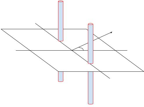
To explain these two aspects, for convenience, let’s use a two-dimensional model by applying a dimensional reduction to the “spherical chicken in a vacuum.” We will consider the beam pattern of the “rod” antenna commonly used in Wi-Fi routers in the horizontal direction.
Imagine looking down from above at the horizontal plane around the antenna shown in the previous image. In this overhead view, the antenna appears as a small circle. If the antenna radiates uniformly in all horizontal directions, its beam pattern on the horizontal plane would look like the following image:
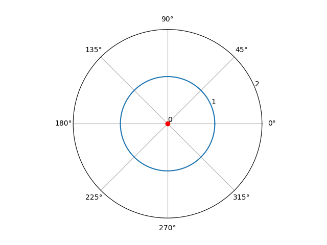
In the diagram, the range from 0 to 360 degrees represents the various directions indicated by the theta angle in the previous image. The red circle at the center is how the antenna appears in the overhead view, and the number 1 on the blue circle indicates that the radiation strength is 1 in all theta angle directions. The value 1 can be understood as an ideal reference unit (corresponding to a gain of 0dB, but due to losses, it generally doesn’t reach 0dB; for simplicity, we’ll ignore the losses for now). The command to draw the above result is as follows:
git clone https://github.com/JiaoXianjun/sdrfun.git
cd sdrfun/beamforming/python/
python3 -c "from beamforminglib import *; ant_array_beam_pattern(freq_hz=2450e6, array_style='linear', num_ant=1, ant_spacing_wavelength=0.5)"
The parameters mean: 2.45GHz carrier frequency, linear array, 1 antenna, antenna spacing of 0.5 wavelength.
Let’s add a second antenna, with the two antennas spaced 6.1cm apart, which is half the wavelength of the 2.45GHz frequency electromagnetic wave:
Then the beam pattern produced by these two antennas would look like the following image:
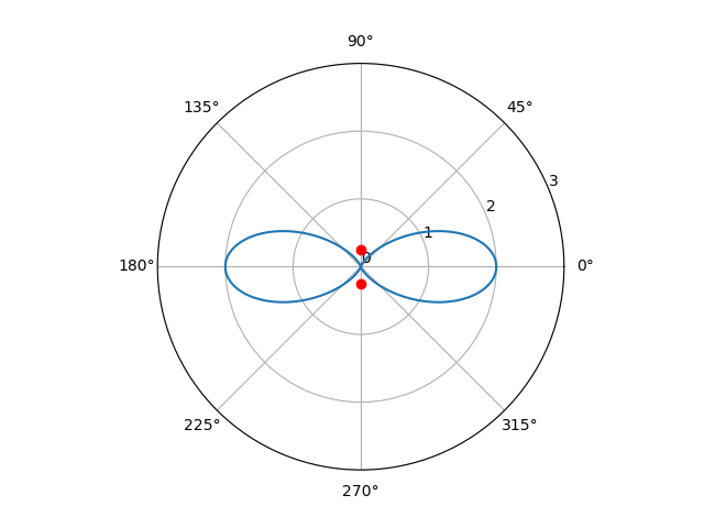
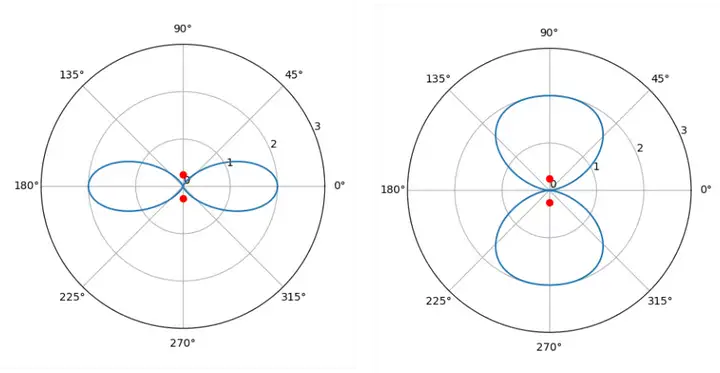
As can be seen, in the 0 and 180 degree directions, the radiation from the antennas has doubled, going from 1 to 2 (which corresponds to a 3dB gain), while in the 90 and 270 degree directions, the radiation disappears, becoming 0. The beam pattern seems an “8” shape. The corresponding command to draw the result (the only changed parameter is the number of antennas, from 1 to 2) is as follows:
python3 -c "from beamforminglib import *; ant_array_beam_pattern(freq_hz=2450e6, array_style='linear', num_ant=2, ant_spacing_wavelength=0.5)"
This is quite interesting. While the addition of multiple antennas is intended to improve the signal, it unexpectedly makes the signal worse in some directions (the directions where the blue “8” shape is less than 1). It seems that effectively using multiple antennas in Wi-Fi routers is not easy/straight-forward, and we’ll discuss the multi-antenna setup of Wi-Fi routers in a later article.
Returning to the “8” shaped beam pattern above, it can actually be easily explained: each antenna still radiates omnidirectionally, but the superposition of the electromagnetic waves from the two antennas in space results in different strengths in different directions. For example, in the 0/180 degree directions, the electromagnetic waves from the two antennas remain strictly in sync with when they left the antennas, because the distance from each point to the two antennas is the same in these directions, meaning the electromagnetic waves from the two antennas maintain the same phase. Imagine two sine waves with the same phase being superimposed; naturally, they become stronger. In the 90/270 degree directions, however, the distance from each point to the two antennas differs by half a wavelength (the antenna spacing), which means there is a 180-degree phase difference, completely opposite. Imagine two sine waves with a 180-degree phase difference being superimposed; of course, they cancel each other out. In the directions between these two, the situation is between the two extremes.
The situation where two sine waves are superimposed with different phases is illustrated in the following image:
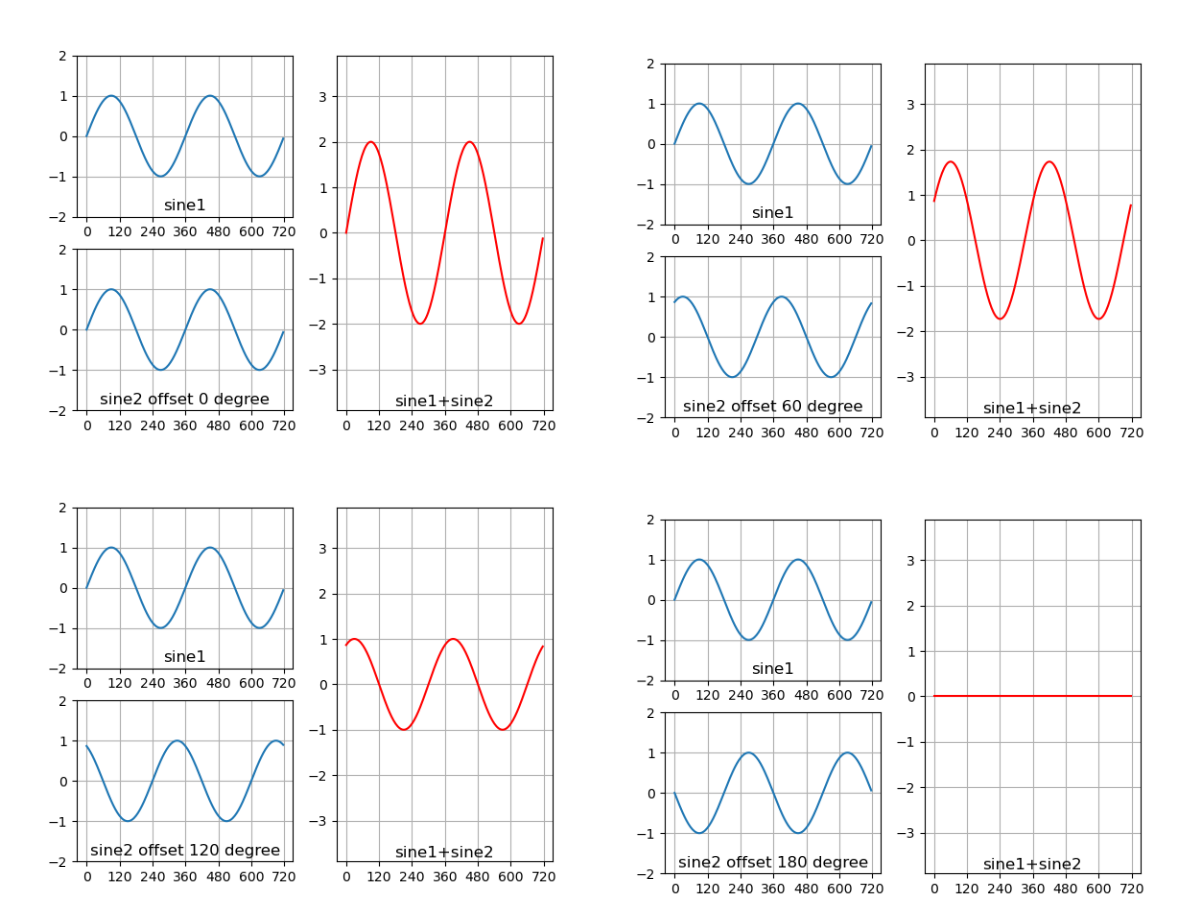
The command to draw the above results is as follows (please manually modify the phase difference parameter offset_degree in the script):
python3 test_sine_offset_combine.py
It shows the superposition of two sine waves with phase differences of 0 degrees, 60 degrees, 120 degrees, and 180 degrees, respectively. You can draw the situation with different phase differences by modifying the offset_degree variable in the script test_sine_offset_combine.py.
Now, the question is: using the same radio wave beamforming code, if we set it to the parameters of double-slit interference in the case of light, can we reproduce the double-slit interference of light? Let’s start experimenting.
(To be continued …)
]]>The open-source BTLE (Bluetooth Low Energy) baseband chip design
Xianjun Jiao, 2024.
SPDX-FileCopyrightText: 2024 Xianjun Jiao
SPDX-License-Identifier: Apache-2.0 license
- [Summary of reference projects and papers]
- [Summary of the version of main packages]
- [BTLE chip architecture]
- [The overall design and implementation methodology]
- [Prior arts analysis]
- [Introduction of the reference SDR BTLE project and its users]
- [Basic principle of BTLE algorithm and structure of the project files]
- [Align the Python algorithms to the SDR BTLE project]
- [Use Python script to evaluate BER under different clock error]
- [Use Python script and Verilog testbench to simulate the design]
- [Synthesis and Implementation for Xilinx FPGA]
- [Run through OpenLane2 SKY130 PDK flow to generate GDSII]
Summary of reference projects and papers
| Link | Role |
|---|---|
| https://www.bluetooth.com/specifications/specs/core-specification-5-3/ | Core Specification 5.3 is the main reference. Mainly PartA&B of Vol6: Low Energy Controller |
| https://github.com/JiaoXianjun/BTLE | The starting point. Created ~10 years ago by me. The new design files are in BTLE/python and BTLE/verilog directories |
| https://colab.research.google.com/github/efabless/openlane2/blob/main/notebook.ipynb | The OpenLane2 work flow I learnt/copied |
| https://github.com/halftop/Interface-Protocol-in-Verilog | general_uart is used for HCI (Host Controller Interface) |
| https://github.com/KennethWilke/sv-dpram | Dual port ram in Verilog (modified in this project) |
| https://public.ccsds.org/Pubs/413x0g3e1.pdf | Figure 3-3: GMSK Using a Quadrature Modulator – The GFSK modulation method adopted in this project |
| https://research.utwente.nl/en/publications/bluetooth-demodulation-algorithms-and-their-performance | Fig. 6. Phase-shift discriminator – The GFSK demodulation method adopted in this project |
Summary of the version of main packages
| Packages | Version |
|---|---|
| Ubuntu | 22.04.4 LTS 64bit |
| libhackrf-dev | amd64/jammy 2021.03.1-2 uptodate |
| Icarus Verilog | version 12.0 (stable) (s20221226-498-g52d049b51) |
| cmake | version 3.22.1 |
| build-essential | amd64/jammy 12.9ubuntu3 uptodate |
| Python | 3.10.12 |
| numpy | Version: 1.21.5 |
| matplotlib | Version: 3.5.1 |
| BTLE commit | https://github.com/JiaoXianjun/BTLE/commit/ff4f2cf17e7a7cd91db6326edd24fa7128a5d945 |
| Xilinx Vivado | 2021.1 |
| openlane | 2.0.0rc2 |
| sky130 PDK | bdc9412b3e468c102d01b7cf6337be06ec6e9c9a |
Introduction
The open-source chip design is a hot topic in recent years. Across big companies to enthusiasts, lots of efforts have been put in multiple domains: high level instruction set definition (RISC-V), new HDL (Hardware Description Language, such as Chisel and SpinalHDL), open chip design (Rocket, BOOM), open EDA (Electronic Design Automation) tools (Yosys, OpenLane) and open PDK (Process Design Kit, such as SkyWater 130). These efforts inspired many active projects in the area of CPU (Central Processing Unit) and MCU (Micro Controller Unit) design. However open-source designs in the radio connectivity domain remain scarce. This project, the open-source BTLE (Bluetooth Low Energy) baseband chip design, aims to establish a foundational project in the domain of open radio connectivity chip design. Regarding the difference between this project and some prior arts, please find the prior art analysis section. As far as I know, this is the 1st open-source BTLE baseband project, that covers all modules from PDU to IQ sample, written in Verilog.
The main features and innovative points of this design are:
- Sub set of BTLE core spec v5.3
- LE 1M, with uncoded data at 1 Mb/s
- GFSK (Gaussian Frequency Shift Keying) with BT(Bandwidth-bit period product)=0.5
- Modulation index 0.5
- Preamble has 1 octet
- Access address has 4 octets
- PDU (Protocol Data Unit) has 2-39 octets
- CRC (Cyclic Redundancy Check) has 3 octets
- BER (Bit Error Rate) performance
- With max 50PPM clock error, BER 0.1% @ 24.5dB SNR
- With 20PPM clock error, BER 0.1% @ 11.5dB SNR
- Configurable gauss filter taps – Flexible bandwidth/spectrum-shape
- Support non-standard BT value or other phase smoothing strategy, such as GMSK (Gaussian Minimum Shift Keying).
- Configurable COS and SIN table – Flexible modulation index
- Support non-standard frequency deviation
- 16MHz main clock speed. 8x oversampling in both transmitter and receiver
- oversampling rate is customizable in design time
The rest part of the document is organized into these sections:
- BTLE chip architecture
- The overall design and implementation methodology
- Prior arts analysis
- Introduction of the reference SDR BTLE project and its users
- Basic principle of BTLE algorithm and structure of the project files
- Align the Python algorithms to the SDR BTLE project
- Use Python script to evaluate BER under different clock error
- Use Python script and Verilog testbench to simulate the design
- Synthesis and Implementation for Xilinx FPGA
- Run through OpenLane2 SKY130 PDK flow to generate GDSII
BTLE chip architecture
(It is assumed that the audiences already have basic knowledge of BTLE. If not, please check quickly the references in the SDR BTLE project: https://github.com/JiaoXianjun/BTLE/tree/master/doc)
Introduce what does the “BTLE chip” mean:
- BTLE core spec v5.3 Vol1 PartA Section2: “The Bluetooth Core system consists of a Host and a Controller”.
- Vol4, HCI (Host Controller Interface) is defined over several options, such as UART (Universal Asynchronous Receiver-Transmitter), USB (Universal Serial Bus), etc.
- Vol6, the LE (Low Energy) Controller is composed of Physical Layer and Link Layer.
- The Physical Layer is responsible for GFSK modulation/demodulation till RF (Radio Frequency) and antenna.
- The Link Layer includes: packet composing/decomposing; control logic (protocol).
- In this project, BTLE chip refers to the LE controller.
This project implements the LE controller that has Physical Layer and Link Layer, except that:
- ADC(Analog to Digital Converter)
- DAC(Digital to Analog Converter)
- zero-IF (Intermediate Frequency) analog transceiver
In other words, this project focuses on the baseband part, not RF.
The control logic in the Link Layer and the HCI currently are dummy modules due to the limited development time. The dummy module is suitable to be implemented by a simple MCU, such as some RISC-V project.
The overall design and implementation methodology
In this project the open BTLE baseband is implemented in Verilog. The baseband bit-true algorithm model is implemented and verified in Python. The Python scripts are also used to generate test vectors and reference results for Verilog modules. The Python algorithm is based on and aligned with the parent project: BTLE – The open-source SDR (Software Defined Radio) Bluetooth Low Energy, which was created by me about 10 years ago. The SDR BTLE project is written in C language and can communicate with the commercial BTLE devices (Phone, Pad, etc.) via SDR hardwares (HackRF, BladeRF). It works not only in the fixed frequency advertisement channel 37/38/39, but also can track the frequency hopping data channel traffic. This means the completeness of the protocol implementation is high in the reference SDR BTLE project. The Python scripts functionalities are aligned with the SDR BTLE project, so the Python scripts are trustworthy. The Verilog testbench takes the test vectors and the reference result vectors generated by Python scripts, and simulate the functionality of the whole design in iverilog, so the Verilog design’s correctness is guaranteed. The SDR BTLE C program, the Python scripts and the Verilog testbench exchange the test vectors and reference results via files in the operating system. You will see this validation chain throughout this document later on.
Prior arts analysis
-
Bluetooth Low Energy Baseband, 2018, is a classroom project. It is written in Chisel, and only includes the bit level processing (scrambling and CRC) of the LE Link Layer. GFSK modulation and demodulation is not included. It is far from a complete LE baseband.
-
Low Power Bluetooth Baseband with a RISC-V Core for Autonomous Sensors using Chisel, 2022-10-13, is a master thesis work that writes some BTLE baseband functionalities in Chisel. Like the previous classroom project, this project also mainly implements the bit level processing (scrambling and CRC). GFSK modulation and demodulation is not included. It is far from a complete LE baseband.
-
A Bluetooth Low Energy Radio using FPGA SERDES: No ADC, AGC, filters, mixers, or amplifiers required., 2021, is the BTLE receiver and transmitter written in nmigen HDL. It has learnt and acknowledged my SDR BTLE project at the end of README. The main unique point of the project is implementing a kind of “Sigma Delta Modulation” with the high speed SERDES differential lines on the FPGA to create an ADC and DAC. It is a kind of experimental work mainly for demonstrating the unique idea of using FPGA SERDES as SDR radio frontend. The full support/testing of every corner of the BTLE protocol is not the main consideration. For example, it supports only fixed preamble and access address patterns for advertisement channels, and does not support the data channel packet transmission and reception. As a comparison, my SDR BTLE project targets to create a full/complete baseband that works not only for advertisement channels but also data channels. Not like the experimental SERDES idea, my project works with the mature zero-IF analog transceiver.
-
A Fully Synthesizable Bluetooth Baseband Module for a System-on-a-Chip, 2003, ETRI Journal, Volume 25, Number 5, October 2003, is for Bluetooth instead of Bluetooth LE (BT classical and LE are different). The paper is only for result reporting, not open sourcing.
Introduction of the reference SDR BTLE project and its users
The SDR BTLE project was created by me about 10 years ago. It implements the BTLE stack in C language and can communicate with the COTS (Commercial Off The Shelf) devices via SDR boards, such as HackRF and BladeRF. The capability includes not only advertisement packet processing in the fixed frequency channel but also data packet in the frequency hopping channels. Since it was created, it has been used in multiple projects and academic papers. This track record brings people confidence if it is the starting point of the open BTLE chip design.
Some example works that are based on my SDR BTLE project:
-
Bidirectional Bluetooth Backscatter With Edges, 2024 IEEE Transactions on Mobile Computing (Volume: 23, Issue: 2, February 2024). In this work the SDR BTLE acts as a core module in the SDR edge server (with HackRF) to setup a bidirectional link between the BTLE reader and the BTLE backscatter tag.
-
Bluetooth Low Energy with Software-Defined Radio Proof-of-Concept and Performance Analysis, 2023 IEEE 20th Consumer Communications and Networking Conference (CCNC). In this work, the USB based SDR devices (such as HackRF, BladeRF) in the SDR BTLE project are replaced by PCIe based SDR devices to achieve the accurate IFS (Inter Frame Space) timing requirement of the BTLE standard. The BTLE stack on the host PC is based on the SDR BTLE project.
-
Tracking Anonymized Bluetooth Devices, 2019, Proceedings on Privacy Enhancing Technologies. This work uses the SDR BTLE project to access the low level raw PHY bit of the BTLE packet, then discovers the vulnerability of BTLE MAC address randomization mechanism. The author says that normally some low level information/PHY-header are discarded by the ASIC/COTS BTLE chip, so SDR is a better choice for BTLE security research. The counter measure was also proposed.
-
Snout: A Middleware Platform for Software-Defined Radios, 2023, IEEE Transactions on Network and Service Management (Volume: 20, Issue: 1, March 2023). This paper implemented a middleware platform that supports many SDR programs and platforms. the btle_rx program (the receiver program in the SDR BTLE project package) is integrated as a receiver example.
-
Bluetooth Low Energy Receiver of portapack-mayhem, 2023. At the end of the page, it says Reference Code Used in Porting Protocol: https://github.com/JiaoXianjun/BTLE . The Portpack is a very popular “HAT” that can be integrated with HackRF SDR board, and run the SDR fully in embedded/hand-held style. The firmware has integrated lots of SDR applications. The BTLE application is based on my SDR BTLE project.
-
Unveiling IoT Vulnerabilities: Exploring Replay Attacks on BLE Devices, 2024. In this experiment, the btle_tx program (the transmitter program in the SDR BTLE project package) is used to generate the attack packet. The purpose is using the SDR device to pretend any other BTLE devices.
-
Security Fuzz Testing Framework for Bluetooth Low Energy Protocols, 2019, Communications of the CCISA, Regular Paper, (Vol 25, No 1, Feb 2019), TAIWAN. This paper integrates the btle_tx program for fuzzing (malformed) packet generation in their BTLE fuzzing test framework.
-
Bluetooth Security, 2018, Book Chapter, pp 195-226, First Online: 20 March 2018. In this chapter of the book “Inside Radio: An Attack and Defense Guide”, the SDR BTLE project is introduced as a tool for security research.
Basic principle of BTLE algorithm and structure of the project files
According to the section of “BTLE chip architecture”, the BTLE chip actually refers to the LE controller. The controller is composed of two modules: Link Layer and Physical Layer. The following figure shows the big picture of BTLE operation principle, and involved modules with Verilog file name in blue (Python function names are similar). It also shows what is included in this project and what is not included. To check how each module work, please refer to seciont “Use Python script and Verilog testbench to simulate the design”
According to the standard, the Link Layer includes the control logic and packet composition/decomposition part. The Physical Layer does the GFSK modulation/demodulation till RF and antenna. The following further elaboration on the operation principle is based on the reference SDR BTLE project, the standard (core spec v5.3) and some other references. The principle is also shown in the above figure.
The packet composition, also called bit level processing, does the CRC24 calculation and pad the 3 CRC octets to the original PDU. Then scramble the PDU to get Physical Layer bits. Before sending it to GFSK modulation in Physical Layer, preamble (1 octet) and access address (4 octets) are padded before the scrambled PDU bit. According to the standard, the scrambling pattern and the preamble is related to the channel number. The CRC initial state and the access address are either fixed (advertisement channel) or negotiated with peers (data channel).
The Physical Layer GFSK modulation’s principle could refer to the “Figure 3-3: GMSK Using a Quadrature Modulator” in CCSDS 413.0-G-3. The basic idea of the implementation is that: bit 0 will drive the input address decrementing for the phase (COS and SIN) table to generate negative frequency deviation; bit 1 will drive the input address incrementing for the phase table to generate positive frequency deviation. The 0-1 transition smoothing is controlled by the coefficients of gauss filter, and this further shapes the spectrum. The max positive/negative frequency achieved is controlled by the waveform samples in the COS&SIN table. In this project, both gauss filter coefficients and COS&SIN table are configurable. This will help the design support multiple standards/purpose beyond BTLE.
The packet decomposition in the Link Layer at the receiver side does the inverse bit level processing of that in the transmitter. It is trivial.
The GFSK demodulation in the Physical Layer at the receiver side uses a simple Signal-to-Bit algorithm (digital baseband version of Fig.6 in https://research.utwente.nl/en/publications/bluetooth-demodulation-algorithms-and-their-performance):
sign(i0*q1-i1*q0).
Where sign() means taking the sign of the result. Positive means 1, negative means 0. i0, q0, i1, q1 are input IQ samples at two successive sampling moments spaced by 1us (according to the LE 1M PHY in the standard)
Above actually detects whether the phase rotates clockwise or counter-clockwise between two successive IQ samples. It starts from:
(i1+q1*j)*conj(i0+q0*j) = i1*i0+q1*q0+(i0*q1-i1*q0)*j
It is easy to understand that the sign of the imaginary part i0*q1-i1*q0 decides the rotation direction.
In our design, 8x oversampling is used in both transmitter and receiver. But the receiver does not know which one out of 8 sampling phases is the best after the signal experiences the circuit/channel propagation delay and the noise. So the receiver will do the GFSK demodulation and inverse bit level processing on all 8 sampling phases, and output the one that gives correct CRC checksum. The oversampling rate is also configurable.
In this project, the HCI UART interface between the controller Link Layer and the host is forked from https://github.com/halftop/Interface-Protocol-in-Verilog . The Link Layer control logic is temporarily a dummy module due to limited development time. In principle, the control logic module can be implemented by some simple RISC-V core.
The project includes two self explaining directories: python and verilog. The naming of those files are well aligned with the BTLE operation principle introduced above.
For Python files,
- btlelib.py has the top level transmitter function btle_tx and receiver function btle_rx. It also has all the sub-functions and some other helper functions, such as clock error emulation and AWGN (Additive White Gaussian Noise) channel.
- btle_tx’s subfunctions: crc24, crc24_core, scramble, scramble_core, gfsk_modulation_fixed_point, vco_fixed_point, etc.
- btle_rx’s subfunctions: gfsk_demodulation_fixed_point, search_unique_bit_sequence, scramble, scramble_core, crc24_core, etc.
- test_alignment_with_btle_sdr.py compares the signal generated by the Python transmitter (by calling btle_tx) and the signal generated by the SDR BTLE project.
- test_btle_ber.py simulates the BER vs SNR (Signal to Noise Ratio) under specified clock frequency error (max 50PPM according to the standard). It calls btle_tx, AWGN channel, cock error emulation, btle_rx, and runs many PDUs to get reliable BER statistics.
- test_vector_for_btle_verilog.py generates test vectors and the reference result vectors for Verilog testbench by using a similar script like test_btle_ber.py. The main difference is that it turns on the file saving flag.
For Verilog files,
- btle_controller.v is the top level module.
- btle_controller.v has Link Layer module btle_ll.v (with dummy control logic) and btle_phy.v, which actually include the Link Layer bit level processing and Physical Layer GFSK modulation and demodulation.
- btle_phy.v has btle_tx.v and btle_rx.v for transmitter and receiver respectively. btle_tx.v is matched to the btle_tx function in btlelib.py. btle_rx.v is matched to the btle_rx function in btlelib.py.
- btle_tx.v has submodules which are well aligned with the phython functions.
- btle_rx.v has 8 bele_rx_core.v instances via the “generate” method of Verilog to act as 8 parallel decoders working on 8 different sampling phases. Any of the 8 decoders has the correct CRC, the receiver will end working on the current packet. There is also a timeout logic to ensure the receiver will not work endlessly.
- btle_rx_core.v has submodules which are well aligned with the phython functions.
- module/submodule specific Verilog testbench file is module_name_tb.v.
- Though the top level module btle_controller.v has a UART interface, currently the UART is not used. The testbench btle_controller_tb.v uses the exposed raw Link Layer bit interface passing through the dummy Link Layer control logic.
Align the Python algorithms to the SDR BTLE project
(If you don’t like local installation, just upload and run open_btle_baseband_chip.ipynb in google colab. This readme is for local setup.)
Install necessary libs, download the open BTLE chip design (python and verilog directory) and build the reference SDR BTLE project.
sudo apt install libhackrf-dev
sudo apt install iverilog
git clone https://github.com/JiaoXianjun/BTLE.git
cd BTLE/host/
mkdir -p build
cd build/
cmake ../
make
You should see messages of successful builing like:
...
[ 75%] Building C object btle-tools/src/CMakeFiles/btle_rx.dir/btle_rx.c.o
[100%] Linking C executable btle_rx
[100%] Built target btle_rx
Run SDR BTLE project to generate IQ sample of a BTLE packet and save it to phy_sample.txt
cd ../../python/
../host/build/btle-tools/src/btle_tx 10-LL_DATA-AA-11850A1B-LLID-1-NESN-0-SN-0-MD-0-DATA-XX-CRCInit-123456
Do not worry about the failure due to lacking hardware.
Run test_alignment_with_btle_sdr.py to call Python algorithm generating IQ sample, then calculate realtime frequency offset for the SDR BTLE generated signal (phy_sample.txt) and the Python generated signal (by calling btle_tx in btlelib.py). Save the frequency offset result to btle_fo.txt and python_fo.txt for further plotting and comparison.
python test_alignment_with_btle_sdr.py 2
You should see outputs like:
argument: example_idx
2
Plese run firstly:
../host/build/btle-tools/src/btle_tx 10-LL_DATA-AA-11850A1B-LLID-1-NESN-0-SN-0-MD-0-DATA-XX-CRCInit-123456
and figure like:
Please noticed that “2” is given as argument to the script. It means the example index is 2. The Python script also gives hint of this example related btle_tx command line ../host/build/btle-tools/src/btle_tx 10-LL_DATA-AA-11850A1B-LLID-1-NESN-0-SN-0-MD-0-DATA-XX-CRCInit-123456. This command has run before. Though hardware does not exist, the IQ sample is still generated and saved to phyt_sample.txt. The command also shows some information during the packet generation:
...
before crc24, pdu
0100
after crc24, pdu+crc
01009b8950
after scramble, pdu+crc
9bc14d4c14
...
The argument 10-LL_DATA-AA-11850A1B-LLID-1-NESN-0-SN-0-MD-0-DATA-XX-CRCInit-123456 given to btle_tx means that it is a data packet in channel 10 with access address 0x11850A1B and CRC initial state 0x123456. Regarding the exact meaning of the argument of btle_tx, please refer to the project README https://github.com/JiaoXianjun/BTLE/blob/master/README.md
If you open the test_alignment_with_btle_sdr.py and find out the initialization code for example 2, you will see
print('Plese run firstly:')
print('../host/build/btle-tools/src/btle_tx 10-LL_DATA-AA-11850A1B-LLID-1-NESN-0-SN-0-MD-0-DATA-XX-CRCInit-123456')
channel_number = 10 # from the 1st field in above btle_tx command argument
access_address = '1B0A8511' # due to byte order, the 11850A1B in above argument needs to be 1B0A8511
crc_state_init_hex = '123456' # from the CRCInit field in above btle_tx command argument
crc_state_init_bit = bl.hex_string_to_bit(crc_state_init_hex) # from the CRCInit field in above btle_tx command argument
pdu_bit_in_hex = '0100' # from the output of above btle_tx command
These are aligned with the argument and output of btle_tx program. This is the way of how SDR BTLE and phython take the same input. Only when the input are the same, comparison of the output is meaningful.
In the above figure the Python btlelib.py output (red) is well aligned with the SDR BTLE btle_tx output. The minor differences happen at the ramping up area (at the beginning) and the max frequency deviation area (around +/-0.25). It is due to the fact that the Python scripts use slightly different oversampling rate, gauss filter coefficients and COS&SIN table. But they both meet the BTLE standard requirements.
On page 2641 of the BTLE core spec v5.3, it says “The minimum frequency deviation shall never be less than 185 kHz when transmitting at 1 megasymbol per second (Msym/s) symbol rate”. The above figure shows the normalized frequency offset with regards to 1Msym/s. The normalized frequency offset of 185kHz is 185KHz/1Msym/s = 0.185. In the figure, the max frequency deviation during each bit period is always bigger than 0.2 which is larger than the minimum requirement 0.185 in the standard.
Now let’s run example 0 which has a longer packet in advertisement channel number 37.
../host/build/btle-tools/src/btle_tx 37-DISCOVERY-TxAdd-1-RxAdd-0-AdvA-010203040506-LOCAL_NAME09-SDR/Bluetooth/Low/Energy r500
Then run test_alignment_with_btle_sdr.py with example index 0 and compare the Python and SDR BTLE result. Again they are aligned.
python test_alignment_with_btle_sdr.py 0
Use Python script to evaluate BER under different clock error
After we have verified Python btle_tx model/algorithm, the corresponding Python receiver algorithm is designed and implemented in btlelib.py. Please find the basic idea of the receiver algorithm in the section “Basic principle of BTLE algorithm and structure of the project files”
Then the next step is evaluating the BER (Bit Error Rate) performance of the receiver algorithm before going to the Verilog implementation. The BER performance is mainly affected by the AWGN noise, clock frequency error between the transmitter and the receiver. The multipath effect is not dominant here because the BTLE is basically a narrow band system. The related requirements in the standard (core spec v5.3) are listed:
- “3.1 MODULATION CHARACTERISTICS: The symbol timing accuracy shall be better than ±50 ppm.”
- “4 RECEIVER CHARACTERISTICS: The reference sensitivity level referred to in this section is -70 dBm”
- “4.1 ACTUAL SENSITIVITY LEVEL: Maximum Supported Payload Length (bytes) 1 to 37, BER 0.1%. LE Uncoded PHYs, Sensitivity (dBm) <= -70”
For nowadays hardware quality, the above requirement is not tough. The crystal could reach PPM performance well below 50PPM easily. At -70dBm RSSI (Received Signal Strength Indicator) level, SNR could reach above 25dBm easily.
The Python script test_btle_ber.py constructs the simulation chain of btle_tx, AWGN channel and clock error emulation, btle_rx and BER statistics. It runs 300 packets with random content to achieve stable BER results. The packet has the maximum 37 octets in the PDU payload field, and 39 octets (2 octet header) in total for the PDU. It means 300*39*8 = 93600 bits passing through at each SNR point. There will be 93.6 error bits for BER 0.1%. Normally having around 100 error bits is regarded as sufficient.
Now let’s run a worst 50PPM case by giving 50 as argument to the test_btle_ber.py, and plot the BER-SNR curve. It will take a while.
python test_btle_ber.py 50
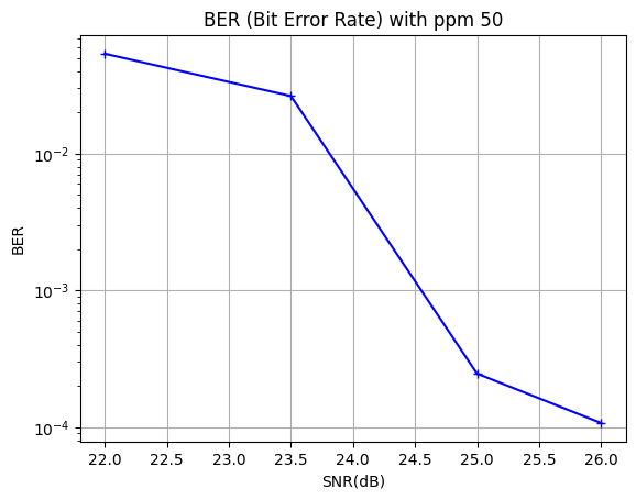
During the simulation, some realtime info is shown: ppm value, frequency offset (50PPM –> 122.5KHz under 2.45GHz center frequency of 2.4GHz ISM band), BER and related the number of error bits, etc.
The figure shows that BER 0.1% is achieved around SNR 24.5dB, which is easy to have with RSSI -70dBm. This means the receiver algorithm meets the standard requirements on BER/sensitivity.
Let’s simulate another better case: -30PPM.
python test_btle_ber.py -30
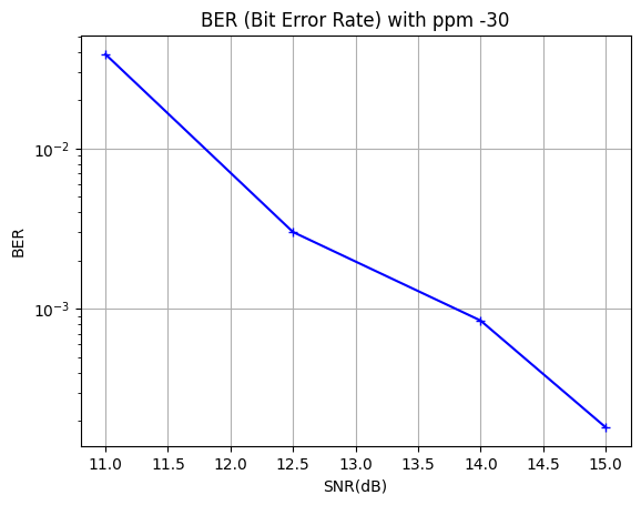
From the above figure, BER 0.1% is achieved around SNR 13.5dB. In modern hardware, 30PPM is an easy task for a crystal, and it already can bring big gain on the sensitivity.
Use Python script and Verilog testbench to simulate the design
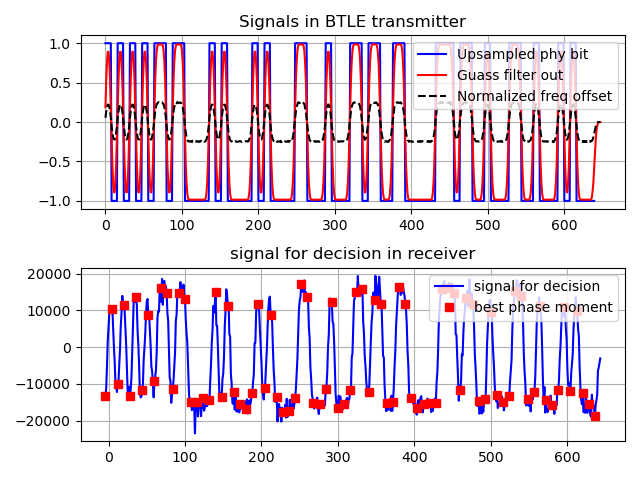
Run test_vector_for_btle_verilog.py to generate test vectors and reference results into the verilog directory. The script also shows the input and output waveforms of some key Python/Verilog modules.
python test_vector_for_btle_verilog.py 2
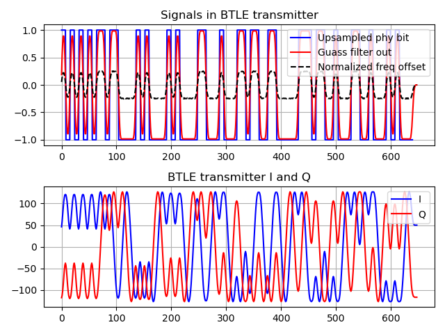
In above example, “2” is input as argument to test_vector_for_btle_verilog.py. It is the same example index as introduced in the section “Align the Python scripts to the SDR BTLE project”.
The full argument list for test_vector_for_btle_verilog.py is: example_idx snr ppm_value num_sample_delay. The name is self explained.
The figure shows that:
- The upsampled PHY bit (PDU bit after CRC and scramble), which is in blue squared NRZ waveform, is shown in the top figure.
- After the gauss filter, the PHY bit NRZ waveform is smoothed, and shown in red.
- Then the gauss filter output drives the GFSK modulator to generate the IQ (COS, SIN) sample which is shown as I (red) and Q (blue).
- The IQ sample related normalized frequency offset is shown in the dashed black curve in the top figure. It is well aligned with the PHY bit and gauss filter output waveform.
- The bottom figure shows the output of GFSK demodulator (algorithm:
sign(i0*q1 - i1*q0)) in blue, and the best sampling phase (out of 8 possible phases) that gives correct CRC, in red square.
Now let’s run the top level Verilog testbench btle_controller_tb.v which takes the Python transmitter input&output and the Python receiver input&output as test vectors.
cd ../verilog/
iverilog -o btle_controller_tb btle_controller_tb.v btle_controller.v btle_ll.v uart_frame_rx.v uart_frame_tx.v rx_clk_gen.v tx_clk_gen.v btle_phy.v btle_rx.v btle_rx_core.v gfsk_demodulation.v search_unique_bit_sequence.v scramble_core.v crc24_core.v serial_in_ram_out.v dpram.v btle_tx.v crc24.v scramble.v gfsk_modulation.v bit_repeat_upsample.v gauss_filter.v vco.v
vvp btle_controller_tb
You should see outputs like:
...
rx Save output to                                                   btle_rx_test_output.txt
rx crc_ok flag verilog 1 python 1
rx Test PASS.
rx compare the btle_rx_test_output_mem and the btle_rx_test_output_ref_mem ...
rx           0 difference found
TEST FINISH.
tx test_ok 1
rx test_ok 1
btle_controller_tb.v:605: $finish called at 391031250 (1ps)
Notice that the testbench also emulates the configuration behaviors (before sending packet) to show the runtime flexibility, such as writing the gauss filter coefficient memory and COS&SIN table, that were generated by Python scripts, into the related memory areas inside the controller.
The Verilog testbech btle_controller_tb.v compares the Verilog output with the reference Python output and gives PASS/FAIL indication at the end. From the above testbench output, the test result is PASS.
The testbench of almost all submodules, that compose the BTLE controller, are offered:
- crc24_tb.v
- scramble_tb.v
- bit_repeat_upsample_tb.v
- gauss_filter_tb.v
- vco_tb.v
- gfsk_demodulation_tb.v
- search_unique_bit_sequence_tb.v – here the unique bit sequence is referring to the access address
- btle_rx_core_tb.v
- btle_tx_tb.v
- btle_rx_tb.v
At the beginning of each Verilog module_tb.v file, there are detailed instructions about how to generate the test vectors and run the testbench.
Some submodule testbench examples will be shown in the following part.
Run the CRC 24 testbench:
iverilog -o crc24_tb crc24_tb.v crc24.v crc24_core.v
vvp crc24_tb
Outputs:
VCD info: dumpfile crc24_tb.vcd opened for output.
WARNING: crc24_tb.v:46: $readmemh(btle_config.txt): Not enough words in the file for the requested range [0:31].
CRC_STATE_INIT_BIT 123456
Reading input from                                      btle_tx_crc24_test_input.txt
         56 read finish for test input.
Reading output ref from                                 btle_tx_crc24_test_output_ref.txt
         80 read finish for test output ref.
         56 input
        80 output
Save output to                                     btle_tx_crc24_test_output.txt
Compare the crc24_test_output_mem and the crc24_test_output_ref_mem ...
          0 error found! Test PASS.
crc24_tb.v:164: $finish called at 86406250 (1ps)
Above testbench shows that 24 bits are padded after the original packet, and the bits are equal to those generated by the Python scripts.
Run the testbench of VCO (Voltage Controlled Oscillator), which has the COS&SIN table as the last stage of GFSK modulator in the transmitter btle_tx:
iverilog -o vco_tb vco_tb.v vco.v dpram.v
vvp vco_tb
Outputs:
VCD info: dumpfile vco_tb.vcd opened for output.
        656 read finish for test input.
Reading output ref from                               btle_tx_vco_test_output_cos_ref.txt
        656 read finish for test output cos ref.
Reading output ref from                               btle_tx_vco_test_output_sin_ref.txt
        656 read finish for test output sin ref.
cos sin table initialized.
        656 input
       656 output
Save output cos to                                   btle_tx_vco_test_output_cos.txt
Save output sin to                                   btle_tx_vco_test_output_sin.txt
Compare the vco_test_output_cos_mem and the vco_test_output_cos_ref_mem ...
          0 error found! output cos Test PASS.
Compare the vco_test_output_sin_mem and the vco_test_output_sin_ref_mem ...
          0 error found! output sin Test PASS.
vco_tb.v:223: $finish called at 214218750 (1ps)
Run the full receiver btle_rx testbench:
iverilog -o btle_rx_tb btle_rx_tb.v btle_rx.v btle_rx_core.v gfsk_demodulation.v search_unique_bit_sequence.v scramble_core.v crc24_core.v serial_in_ram_out.v dpram.v
vvp btle_rx_tb
Outputs:
VCD info: dumpfile btle_rx_tb.vcd opened for output.
WARNING: btle_rx_tb.v:61: $readmemh(btle_config.txt): Not enough words in the file for the requested range [0:31].
CHANNEL_NUMBER 10
CRC_STATE_INIT_BIT 123456
ACCESS_ADDRESS 11850a1b
Reading input I from                                                  btle_rx_test_input_i.txt
        656 read finish for test input I.
Reading input Q from                                                  btle_rx_test_input_q.txt
        656 read finish for test input Q.
Reading output crc_ok ref from                                        btle_rx_test_output_crc_ok_ref.txt
          1 read finish from                                        btle_rx_test_output_crc_ok_ref.txt
Reading output ref from                                               btle_rx_test_output_ref.txt
          2 read finish from                                               btle_rx_test_output_ref.txt
ACCESS_ADDRESS 11850a1b detected
payload_length   0 octet
best_phase idx (among    8 samples) 4
crc_ok 1
        656 NUM_SAMPLE_INPUT
      1456 sample_in_count
Save output to                                                   btle_rx_test_output.txt
crc_ok flag verilog 1 python 1
Test PASS.
Compare the btle_rx_test_output_mem and the btle_rx_test_output_ref_mem ...
          0 difference found
btle_rx_tb.v:232: $finish called at 182406250 (1ps)
Run the gfsk_demodulation (part of the btle_rx receiver) testbench:
iverilog -o gfsk_demodulation_tb gfsk_demodulation_tb.v gfsk_demodulation.v
vvp gfsk_demodulation_tb
Outputs:
VCD info: dumpfile gfsk_demodulation_tb.vcd opened for output.
Reading input I from                                btle_rx_gfsk_demodulation_test_input_i.txt
         82 read finish for test input I.
Reading input Q from                                btle_rx_gfsk_demodulation_test_input_q.txt
         82 read finish for test input Q.
Reading output ref from         btle_rx_gfsk_demodulation_test_output_signal_for_decision_ref.txt
         81 read finish from         btle_rx_gfsk_demodulation_test_output_signal_for_decision_ref.txt
Reading output ref from                         btle_rx_gfsk_demodulation_test_output_bit_ref.txt
         81 read finish from                         btle_rx_gfsk_demodulation_test_output_bit_ref.txt
         82 input
        82 bit output
        82 signal for decision output
Save output bit to                             btle_rx_gfsk_demodulation_test_output_bit.txt
Save output signal for decision to             btle_rx_gfsk_demodulation_test_output_signal_for_decision.txt
Compare the gfsk_demodulation_test_output_bit_mem and the gfsk_demodulation_test_output_bit_ref_mem ...
          0 error found! output bit Test PASS.
Compare the gfsk_demodulation_test_output_signal_for_decision_mem and the gfsk_demodulation_test_output_signal_for_decision_ref_mem ...
          0 error found! output signal for decision Test PASS.
gfsk_demodulation_tb.v:199: $finish called at 112406250 (1ps)
Run the access address searching (part of the btle_rx receiver) testbench:
iverilog -o search_unique_bit_sequence_tb search_unique_bit_sequence_tb.v search_unique_bit_sequence.v
vvp search_unique_bit_sequence_tb
Outputs:
VCD info: dumpfile search_unique_bit_sequence_tb.vcd opened for output.
WARNING: search_unique_bit_sequence_tb.v:43: $readmemh(btle_config.txt): Not enough words in the file for the requested range [0:31].
ACCESS_ADDRESS 11850a1b
Reading input from                 btle_rx_search_unique_bit_sequence_test_input.txt
         81 read finish from                 btle_rx_search_unique_bit_sequence_test_input.txt
Reading output ref from            btle_rx_search_unique_bit_sequence_test_output_ref.txt
          1 read finish from            btle_rx_search_unique_bit_sequence_test_output_ref.txt
unique_bit_sequence full match at the         41th bit
unique_bit_sequence starting idx          9
Compare the unique_bit_sequence starting idx and the search_unique_bit_sequence_test_output_ref_mem[0] ...
Same as python result     9. Test PASS.
         81 input
search_unique_bit_sequence_tb.v:122: $finish called at 111406250 (1ps)
Above Verilog testbench shows that the access address is found at index 9 in the incoming IQ sample stream, and it is equal to the Python script test vector/result. Because the beginning 8 bits are preamble, the access address starts from the 9th bit. We can add 1 sample delay (8 in the oversampling domain) in the channel emulation part of the Python script, and run this access address search testbench again:
cd ../python/
python test_vector_for_btle_verilog.py 2 20 0 8

cd ../verilog/
iverilog -o search_unique_bit_sequence_tb search_unique_bit_sequence_tb.v search_unique_bit_sequence.v
vvp search_unique_bit_sequence_tb
Outputs:
VCD info: dumpfile search_unique_bit_sequence_tb.vcd opened for output.
WARNING: search_unique_bit_sequence_tb.v:43: $readmemh(btle_config.txt): Not enough words in the file for the requested range [0:31].
ACCESS_ADDRESS 11850a1b
Reading input from                 btle_rx_search_unique_bit_sequence_test_input.txt
         82 read finish from                 btle_rx_search_unique_bit_sequence_test_input.txt
Reading output ref from            btle_rx_search_unique_bit_sequence_test_output_ref.txt
          1 read finish from            btle_rx_search_unique_bit_sequence_test_output_ref.txt
unique_bit_sequence full match at the         42th bit
unique_bit_sequence starting idx         10
Compare the unique_bit_sequence starting idx and the search_unique_bit_sequence_test_output_ref_mem[0] ...
Same as python result    10. Test PASS.
         82 input
search_unique_bit_sequence_tb.v:122: $finish called at 112406250 (1ps)
As you can see, the Verilog testbench shows that the access address starts from the index 10 instead of 9 in the previous case, after we add artificial 1 sample delay in the channel.
The argument 2 20 0 8 to test_vector_for_btle_verilog.py means that: example index 2; 20dB SNR; 0 PPM; 8 oversample delay (8 oversample = 1 sample)
Synthesis and Implementation for Xilinx FPGA
Before going to the OpenLan2 in the next section, here we firstly try to map the design into a Xilinx FPGA by Xilinx Vivado 2021.1. Not any paid license is needed because we choose a FPGA model with volume smaller than a certain size. The model is xc7z020 which has been widely used in many FPGA dev boards, such as ZedBoard, PYNQ, etc.
Method to run the Xilinx FPGA project:
- Open Vivado 2021.1, and go to the BTLE/verilog directory by “cd” command in the Tcl Console.
- Run
source ./btle_controller.tclin the Tcl Console to create the project for target FPGA xc7z020 with 16MHz constraints in thebtle_controller_wrapper.xdc - Click
Generate Bitstreamon the left bottom corner to run the FPGA implementation and generate FPGA bitstream.
With the default Xilinx Vivado strategy, the design fits in the FPGA easily without much optimization efforts on the clock speed and area. The main information in the Vivado report:
Utilization:
| Cell | Used | Total in FPGA | Percentage |
|---|---|---|---|
| Slice LUTs | 3563 | 53200 | 6.7% |
| Slice Registers | 2307 | 106400 | 2.1% |
| F7 Muxes | 75 | 26600 | 0.28% |
| F8 Muxes | 16 | 13300 | 0.12% |
| Slice | 1180 | 13300 | 8.87% |
| LUT as Logic | 2687 | 53200 | 5% |
| LUT as Memory | 876 | 17400 | 5% |
| DSPs | 48 | 220 | 21.8% |
Timing:
| Worst Negative Slack (WNS) | Total Negative Slack (TNS) | Number of Failing Endpoints |
|---|---|---|
| 27.701 ns | 0 ns | 0 |
Power:
| Total On-Chip Power | Junction Temperature | Thermal Margin | Effective theta JA |
|---|---|---|---|
| 0.12W | 26.4 C(Celsius) | 58.6C (4.9W) | 11.5 C/W |
The final floorplanning&routing result:
Run through OpenLane2 SKY130 PDK flow to generate GDSII
To run through OpenLane workflow, please upload and run open_btle_baseband_chip.ipynb in google colab. The flow is mainly learnt/copied from this reference colab file:
https://colab.research.google.com/github/efabless/openlane2/blob/main/notebook.ipynb
For local setup, please follow https://openlane.readthedocs.io/en/latest/getting_started/index.html
- The GDSII of the btle rx core
Note: Static Timing Analysis (Post-PnR) failed
- The Detailed Placement and CTS of the whole project
Note: Global Routing failed
]]>今天把车卖了10413欧元,7年开了145520km,贬值15587欧元。
-
2016年购入,车初次注册是在2015,当初里程21000km,26000欧从宝马二手车购入。
-
2023年卖出,里程166520km,卖给了wijkopenautos.be,10413欧元,贬值15587欧元。
卖车流程很丝滑:
在线输入车辆信息,给出评估价。然后去线下现场验车,核对无误后,给出最终报价。我的最终报价和在线评估价一模一样,因为我在线输入的信息完全准确,而且车辆状态的确也不错。立刻签订合同,卖车款2~3个工作日到账。车行拆下车牌我来带走。
也找了之前买车的宝马店,以及其他本地的二手车收购商。都很磨唧,只给9000到10000欧元。而且不少地方一听说是柴油车就不收。现在政府正在强推新能源,再差也要汽油车,2030年后一切燃油车都就买不到了。柴油车在2024(还是2027?)年后将会禁止进入城市核心/绿色区。想进也可以,交钱。
我和wijkopenautos.be签订的合同对方是在阿姆斯特丹的公司(但总部在德国)。还是荷兰人会做生意啊!还是德国人懂车啊!
卖车后流程:
-
车牌交给邮局,由邮局去政府注销,(不然每年还要交车辆税),而且没收钱。。。?(会有账单吗?)
-
拿邮局的回执去保险公司取消保险。